Back in December, Dutch tech giant ASML shipped its first High-NA Extreme Ultraviolet (EUV) lithography machine (EXE:5000) to Intel. The $400 million machine will take us to the next tier of chip production with a process node of 2nm and less. The original EUV machines, also made by ASML, were necessary to get chip foundries to manufacture components under 10nm. A lower process node means smaller transistors, meaning more can fit inside a chip. The higher a chip’s transistor count, the more powerful and/or energy efficient it is.
The reason that the EUV machine is so important is that it prints circuitry patterns on silicon wafers that are thinner than human hair. This is required when you are building a chip with billions of transistors inside. The 7nm A13 Bionic SoC, used to power 2019’s iPhone 11 series, contained 8.5 billion transistors. The 3nm A17 Pro used to run the iPhone 15 Pro and iPhone 15 Pro Max sports 19 billion transistors.
The 8 nm resolution of the EXE:5000 means that chipmakers can pack more transistors into a single chip. Smaller transistors are more energy efficient – that means the chips will be able to do more with less.-ASML
The new High-NA EUV machine has a 0.55 numerical aperture (NA) lens giving it a resolution of 8nm compared to the current machines’ resolution of 13nm (.33 NA). This means that the new machines can print transistors 1.7 times smaller resulting in transistor densities 2.9 times larger with a single exposure. The result? More powerful or energy-efficient chips. The new machines can also print 185 wafers per hour, rising to 220 by 2025. That compares to the 160 wafers per hour that can be printed with the current EUV machines.
The current Low-NA EUV machines can produce the same resolution but only after two exposures are made using double patterning. However, there are risks with double patterning including longer production times, and increased risk that a defect will occur. It can also lead to performance variability among manufactured chips.
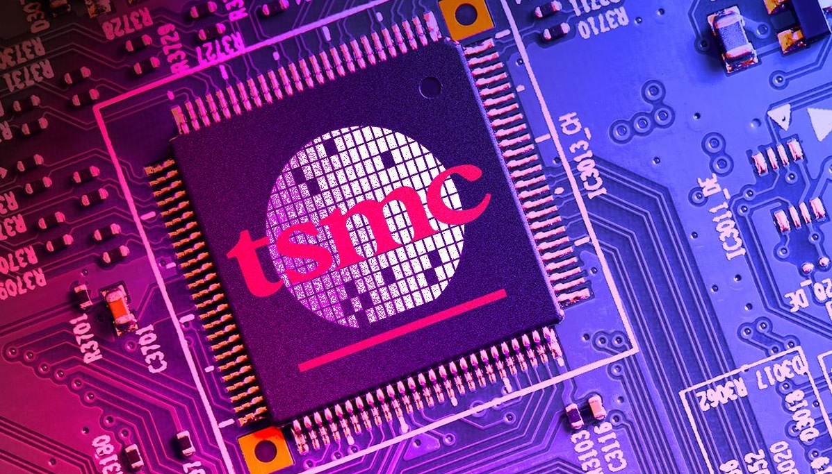
ASML is quick to tell you what can go wrong with double patterning since it would prefer foundries spend the bigger bucks on the newer machines. But TSMC’s N3B process node, which supposedly relies on double patterning, was used to manufacture the A17 Pro application processor used on all of those iPhone 15 Pro and iPhone 15 Pro Max units made by Apple, and the M3 chip used to power high-end Macs. ASML says that its clients are just now doing their research into the High-NA EUV.
Financial institution China Renaissance (via
Eventually, TSMC, Samsung Foundry, and others will have to join Intel and start making the investments needed to move to the High-NA EUV. That time might end up being soon with TSMC and Samsung looking to start 2nm production in 2025 moving to 1.4nm production in 2027.